1.5 mJ / 2 mJ, 355 nm UV Nanosecond Laser
Product Overview
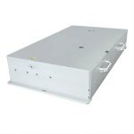
The 355 nm UV Nanosecond Laser is a diode‑pumped solid‑state (DPSS) laser delivering high‑energy UV pulses at 1.5 mJ or 2.0 mJ per pulse, with selectable repetition rates of 6 kHz and 15 kHz. This unique combination of millijoule‑level pulse energy and kilohertz repetition rates bridges the gap between low‑frequency, high‑energy lasers (e.g., 20–50 Hz) and high‑frequency, low‑energy lasers (e.g., >50 kHz). It is ideal for applications that demand both significant per‑pulse energy and moderate‑to‑high throughput, such as precision drilling, via hole formation, wafer scribing, thin‑film ablation, and laser‑induced breakdown spectroscopy (LIBS).
Built on an all‑solid‑state architecture with diode pumping and solid‑state harmonic generation, this laser offers exceptional beam quality, long‑term stability, and maintenance‑free operation – making it a reliable workhorse for 24/7 industrial environments and advanced research laboratories.
Key Features
-
High Pulse Energy – Choose the 1.5 mJ or 2.0 mJ model; both provide ample energy for efficient UV material processing.
-
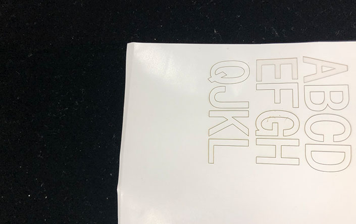
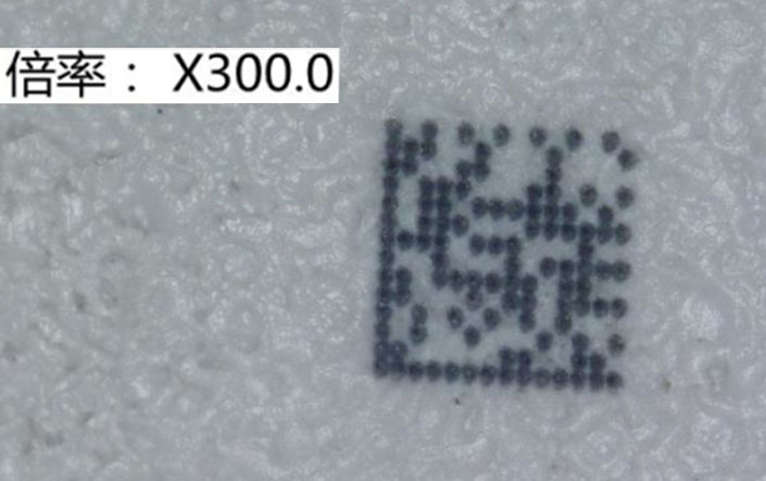
355 nm Deep‑UV Wavelength – Enables high‑resolution patterning, low heat‑affected zone, and strong absorption in semiconductors, glasses, polymers, and ceramics.
-
6 kHz or 15 kHz Repetition Rate – Fixed or field‑selectable models available; allows optimization between higher pulse energy (6 kHz) or higher average power (15 kHz).
-
Nanosecond Pulse Width – < 15 ns (typical 10–12 ns), delivering high peak power for clean ablation and minimal thermal damage.
-
Exceptional Beam Quality – M² < 1.3, circular beam profile, high pointing stability, and near‑diffraction‑limited divergence.
-
All‑Solid‑State Architecture – Diode‑pumped Nd:YAG or Nd:YVO₄ oscillator with solid‑state harmonic conversion (LBO crystals). No flashlamps, no gas refills, no high‑voltage discharge.
-
Industrial Reliability – Sealed laser head, water‑cooled (or optional air‑cooled for lower power), >15,000 hours diode lifetime.
-
Flexible Control – External TTL triggering, internal clock, burst mode, RS‑232 / Ethernet interface, and pulse‑on‑demand capability.
Applications
| Field | Typical Processes |
|---|---|
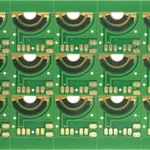
| Electronics Manufacturing | PCB via drilling, flex circuit cutting, ITO scribing, memory repair |
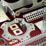
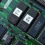
| Semiconductor Processing | Wafer dicing, die marking, laser lift‑off (GaN on sapphire), edge trimming |
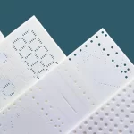
| Precision Micromachining | Glass, sapphire, ceramic drilling and cutting; thin‑film ablation |
| Laser‑Induced Breakdown Spectroscopy (LIBS) | High‑repetition‑rate elemental analysis of metals, glasses, plastics, geological samples |
| Display Industry | OLED panel cutting, TFT array repair, glass edge deletion for LCD |
| Medical Device Manufacturing | Catheter and stent hole drilling; surface structuring of implants |
| Scientific Research | Time‑resolved fluorescence, photoacoustic imaging, pump‑probe spectroscopy, material damage studies |