
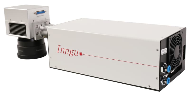
20 mJ / 30 mJ, 351 nm Nanosecond Solid‑State Laser
High‑Energy UV Laser for Precision Material Processing & Advanced Research
Overview
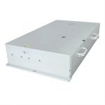
The 351 nm Nanosecond Solid‑State Laser is a diode‑pumped, Q‑switched laser delivering pulse energies of 20 mJ or 30 mJ at a wavelength of 351 nm – the third harmonic of the fundamental 1053 nm (Nd:YLF or Nd:YAG‑based). This high‑energy, nanosecond‑pulsed UV source combines excellent beam homogeneity, long‑term stability, and a compact all‑solid‑state architecture. It is designed for applications requiring deep‑UV photons with sufficient energy per pulse to ablate, modify, or excite materials with minimal thermal damage. From glass cutting and wafer dicing to laser‑induced breakdown spectroscopy (LIBS) and pulsed laser deposition (PLD), this laser provides the power and reliability demanded by both industrial production lines and advanced research laboratories.
Key Features
-
High Pulse Energy – Choose the 20 mJ or 30 mJ model; both provide ample energy for efficient material processing.
-
351 nm Deep‑UV Wavelength – Enables high‑resolution patterning, low heat‑affected zone, and excellent absorption in many materials (semiconductors, polymers, glasses).
-
Nanosecond Pulse Width – Typical 10–15 ns FWHM, delivering high peak power (up to 2–3 MW) for clean ablation.
-
Adjustable Repetition Rate – Operates from single‑shot up to 50 Hz or 100 Hz (model dependent), allowing flexible process control.
-
Excellent Beam Quality – Near‑diffraction‑limited with M² < 1.5, circular beam profile, and high pointing stability.
-
All‑Solid‑State Design – Diode‑pumped gain medium (Nd:YLF or Nd:YAG) with solid‑state harmonic conversion (LBO crystals). No flashlamps, no gas refills, no high‑voltage gas discharge.
-
Industrial Reliability – Sealed laser head, forced air or water cooling, >10,000 hours diode lifetime, and maintenance‑free operation.
-
Flexible Control – External TTL triggering, internal clock, RS‑232/Ethernet interface, and pulse‑on‑demand capability.
Applications
| Field | Application |
|---|---|
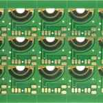
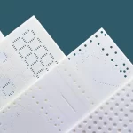
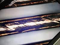
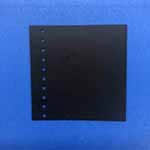
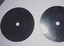
| Precision Micromachining | Glass drilling, sapphire scribing, ceramic cutting, thin‑film ablation |
| Semiconductor | Wafer dicing, die marking, memory repair, GaN lift‑off |
| Laser‑Induced Breakdown Spectroscopy (LIBS) | Elemental analysis of metals, glasses, plastics, and geological samples |
| Pulsed Laser Deposition (PLD) | Thin film growth of oxides, nitrides, and high‑Tc superconductors |
| LIDAR & Remote Sensing | Atmospheric aerosol detection, ozone profiling (351 nm is close to 355 nm but often used in specific systems) |
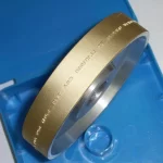
| Medical Device Manufacturing | Hole drilling in catheters and stents; surface structuring of implants |
| Scientific Research | Time‑resolved fluorescence, photoacoustic imaging, pump‑probe spectroscopy, material damage studies |