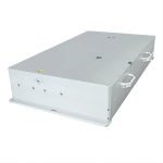
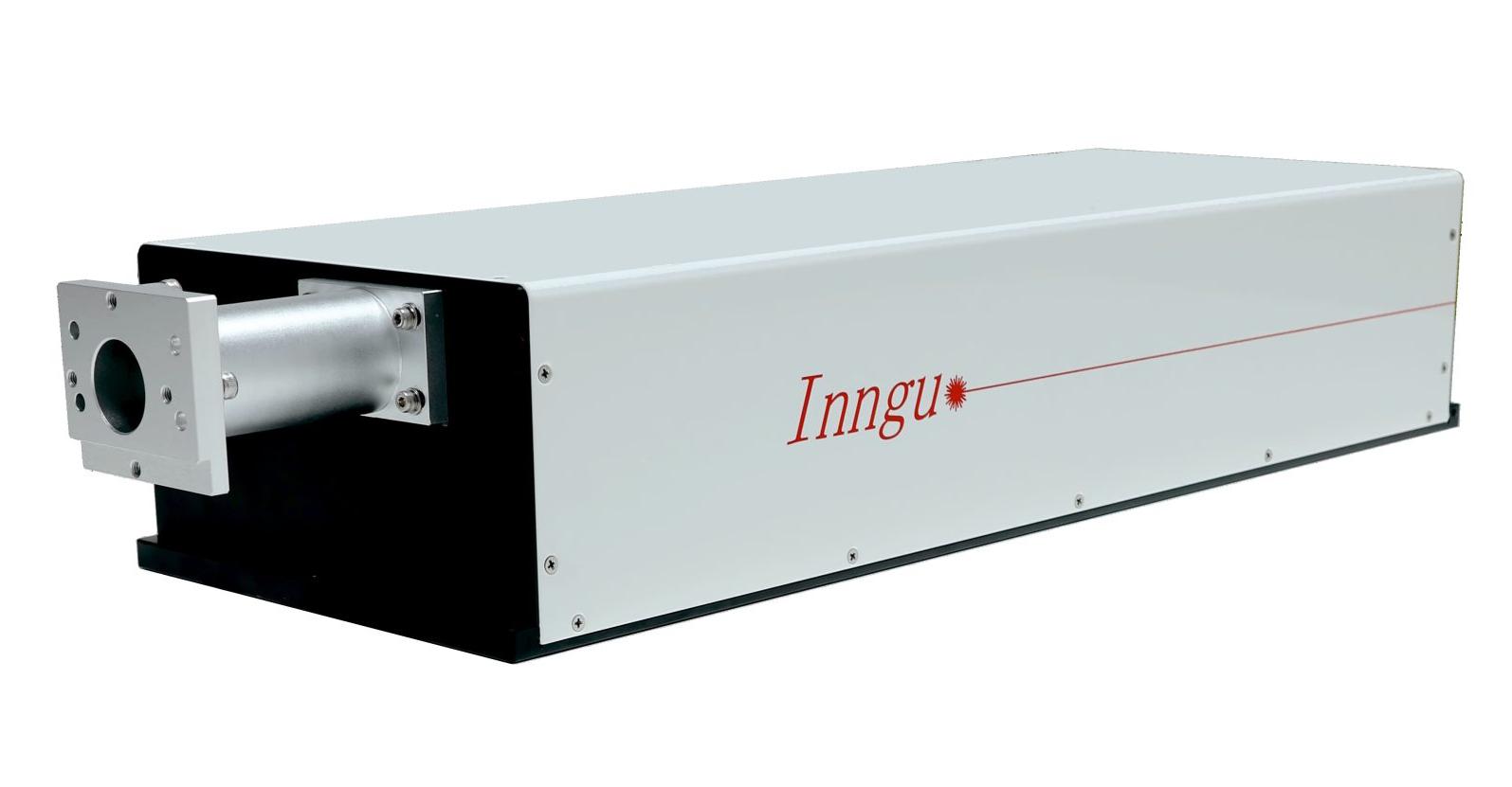
355 nm High Power Nanosecond Solid‑State Laser
Industrial‑Grade UV Laser with All‑Solid‑State Architecture
Product Overview
The 355 nm High Power Nanosecond Solid‑State Laser is a third‑harmonic Nd:YAG (or Nd:YVO₄) laser system that delivers deep‑ultraviolet output with average powers ranging from 10 W to over 100 W. Built on an all‑solid‑state platform – using diode laser pumping and solid‑state harmonic conversion crystals – this laser eliminates gas tubes, flashlamps, and high‑voltage discharge components. The result is a compact, robust, and virtually maintenance‑free UV laser designed for 24/7 industrial operation, precision micromachining, and demanding scientific applications.
Key Features
-
True Solid‑State Design – Diode‑pumped Nd:YAG / Nd:YVO₄ oscillator + solid‑state harmonic generation (SHG + THG). No flashlamps, no gas refills, no high‑voltage spark gaps.
-
High UV Power – Available from 10 W to 100 W (custom up to 150 W) at 355 nm, with excellent power scalability.
-
Nanosecond Pulse Width – Typical 10–25 ns FWHM, providing high peak power for clean, heat‑minimized material processing.
-
High Repetition Rate – Adjustable from 10 kHz to 200 kHz (and beyond), allowing precise control over pulse energy and process speed.
-
Exceptional Beam Quality – M² < 1.3, TEM₀₀ mode, high pointing stability, and circular beam profile.
-
Industrial Reliability – Hermetically sealed, water‑cooled (or optional air‑cooled for lower power models). Diode lifetime > 20,000 hours.
-
Power Stability – < 2% over 8 hours, < 3% over 24 hours, thanks to active temperature control and closed‑loop feedback.
-
Flexible Pulse Control – External TTL triggering, burst mode, pulse‑on‑demand, and internal/external repetition rate control.
Applications
| Industry | Typical Processes |
|---|---|
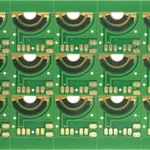
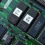
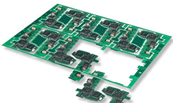
| Electronics Manufacturing | PCB depaneling, flex circuit cutting, ITO scribing, memory repair, wafer dicing |
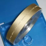
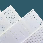
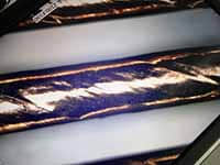
| Precision Micromachining | Drilling, cutting, and structuring of glass, sapphire, ceramics, and thin metal films |
| Semiconductor | Laser lift‑off (GaN on sapphire), die marking, wafer edge trimming |
| Solar Cell Production | Edge deletion, scribiApplications Industry Typical Processes Electronics Manufacturing PCB depaneling, flex circuit cutting, ITO scribing, memory repair, wafer dicing Precision Micromachining Drilling, cutting, and structuring of glass, sapphire, ceramics, and thin metal films Semiconductor Laser lift‑off (GaN on sapphire), die marking, wafer edge trimming Solar Cell Production Edge deletion, scribing of thin‑film solar cells (CIGS, CdTe, a‑Si) Medical Device Fabrication Catheter and stent hole drilling, micro‑cutting of bioresorbable polymers Display Industry OLED panel cutting, TFT array repair, glass edge deletion for LCD Automotive Direct marking of glass and electronic components, fuel injector nozzle drilling Scientific Research LIBS, LIDAR, time‑resolved fluorescence, laser‑induced breakdown spectroscopyng of thin‑film solar cells (CIGS, CdTe, a‑Si) |
| Medical Device Fabrication | Catheter and stent hole drilling, micro‑cutting of bioresorbable polymers |
| Display Industry | OLED panel cutting, TFT array repair, glass edge deletion for LCD |
| Automotive | Direct marking of glass and electronic components, fuel injector nozzle drilling |
| Scientific Research | LIBS, LIDAR, time‑resolved fluorescence, laser‑induced breakdown spectroscopy |