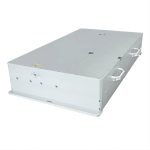
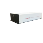


1. Core Definition and Operating Principle
The core of this laser lies in its method of generating optical pulses with these specific parameters. The operating principle typically follows a Master Oscillator Power Amplifier (MOPA) design:
-
Pulse Generation: A stable seed source (e.g., an Nd:YVO₄ crystal or fiber laser) first generates high-quality infrared picosecond (10⁻¹² seconds) pulses.
-
Energy Amplification: These weak seed pulses are then amplified through multiple stages of fiber or solid-state amplifiers. This process significantly boosts their energy while preserving their excellent temporal and beam quality characteristics.
-
Frequency Conversion: The amplified, high-energy infrared light (typically at 1064 nm) is directed through nonlinear optical crystals (such as Lithium Triborate, LBO, or Beta-Barium Borate, BBO). Through efficient third harmonic generation (THG), the wavelength is converted to 355 nm in the UV spectrum.
2. Key Technological Advantages
Compared to traditional long-pulse (e.g., nanosecond) or continuous-wave lasers, the high repetition rate 355 nm UV picosecond laser offers significant physical and technological benefits:
-
Superior “Cold Processing” Effect: The picosecond pulse width is extremely short—much shorter than the lattice vibration time (typically a few picoseconds to tens of picoseconds) during which absorbed light energy is converted into heat in the material. This allows the laser pulse to interact with the material by directly “tearing” electrons away through multiphoton absorption, leading to direct vaporization of the material. This process generates virtually no heat-affected zone (HAZ) or thermal diffusion. Consequently, the processed edges are clean, burr-free, and without micro-cracks, ensuring exceptionally high processing quality.
-
High Precision and Quality: The 355 nm UV photons possess high energy, enabling them to directly break the chemical bonds in many materials (a “photochemical” process) rather than relying solely on thermal effects (“photothermal” process). This characteristic, combined with the ability to focus the UV beam to a very small spot, makes it ideal for processing heat-sensitive materials and applications demanding sub-micrometer precision.
-
High Throughput and Efficiency: A high repetition rate (ranging from tens of kHz to several tens of MHz, or even up to 80 MHz) means a massive number of pulses are delivered per unit time, enabling rapid processing speeds. Coupled with high peak power, this allows for significantly increased processing efficiency. For instance, processing materials like Polyimide (PI) or Indium Tin Oxide (ITO) can be 5 to 10 times faster compared to traditional techniques, leading to a substantial reduction in the cost of ownership (COO) .
Leveraging its unique advantages, this laser is widely adopted across various high-tech fields:
-
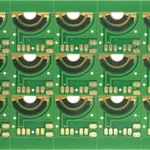
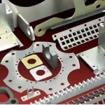
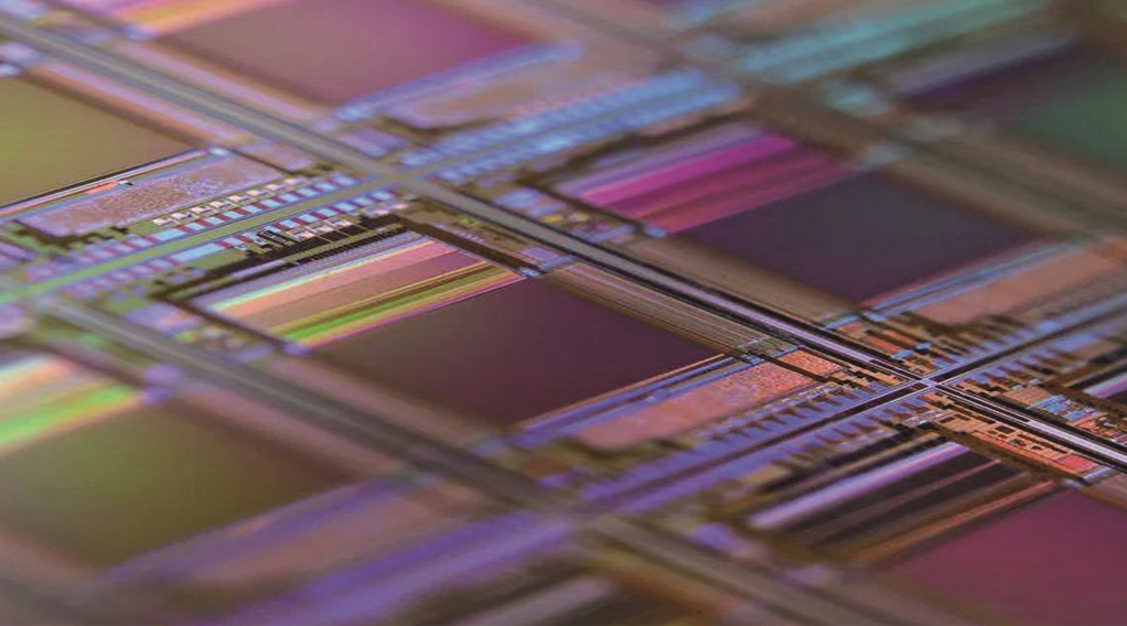
Precision Microelectronics Manufacturing:
-
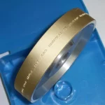
Cutting and drilling of flexible printed circuit boards (FPCB) and substrate-like PCBs (SLP), achieving carbon-free, high-precision results.
-
Precision cutting and drilling of OLED display panels.
-
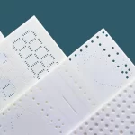
Dicing of semiconductor wafers, especially ultra-thin or brittle ones, to improve chip yield.
-
-
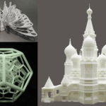
Thin Film and Advanced Material Processing:
-
Ablation and patterning of transparent conductive films (e.g., ITO) on solar cells or flat-panel displays, achieving high speed without damaging the underlying substrate.
-
Processing multi-layer films and materials with low ablation thresholds for fine patterning.
-
-
Scientific Research:
-
Time-resolved spectroscopy: Used to study ultrafast dynamics (e.g., carrier relaxation) in materials on femtosecond to picosecond timescales.
-
Bio-imaging and Microscopy: Serving as a depletion source in STED super-resolution microscopy or for time-resolved fluorescence measurements.
-
The high repetition rate 355 nm UV picosecond laser represents a key direction in advanced laser-based manufacturing. Through the synergistic combination of “UV photons + picosecond pulses + high repetition rate,” it achieves a nearly “cold,” high-quality, and efficient process for fine material structuring. It stands as an essential tool driving innovation in the semiconductor, consumer electronics, display industries, and cutting-edge scientific research.