
As a supplement to traditional material processing methods, laser processing has gradually developed and matured in the field of material processing. The interaction between laser and substance is the physical basis of laser processing. Because the laser must be absorbed and transformed by materials, it can be processed with lasers of different wavelengths, different power densities or different energy densities. The interaction between laser and substance involves a wide range of disciplines such as laser physics, atomic and molecular physics, plasma physics, solid state and semiconductor physics, materials science and etc. When the laser works on the material, electromagnetic energy is initially converted into electron excitation energy and then further converted into heat, chemical energy and mechanical energy. Therefore, during the processing process, various changes will occur in the processed area of the material, mainly reflected in the heating, melting, vaporization of materials and the generation of plasma clouds.
Laser processing refers to the material processing by laser beam such as cutting, welding, surface treatment and drilling. As an advanced manufacturing technology, laser processing has been widely used in the industries of automotive, aviation, electronic and electrical appliances, metallurgy and machinery manufacturing.
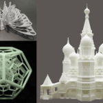
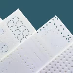
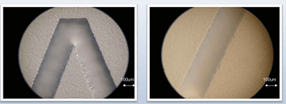
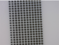
Pulsed laser has obvious advantages in the processing of glass, ceramics and thin metals. With the maturity of laser technology, plenty of different pulsed lasers are being used in the field of micromachining of materials. Generally speaking, the shorter the pulse width of laser is, the better the processing results and the fewer the processing defects or burrs are. However, the price of the laser will be exponentially increased with the pulse width of the laser becomes shorter.
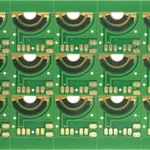
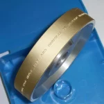
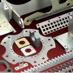
There are many types of lasers which can be divided into gas laser, solid state laser, semiconductor laser and liquid laser according to working substance. Carbon dioxide laser as a kind of gas laser is commonly used for cutting and marking of leather, wood, acrylic and fabric. Because of cost advantages, rich varieties of wavelengths and increased power, semiconductor laser has gradually replaced traditional CO2 or fiber laser in the fields of plastic welding, wood cutting and marking. Fiber laser is currently the most widely used laser and has an important market in the marking of plastics, wood and metal materials as well as in the rust removal, welding and cutting of metals. Semiconductor pumped solid state laser has obvious advantages in non-metallic materials, such as marking, engraving and cutting of glass, fine marking of plastic or semiconductor materials and processing and manufacturing of PCB.
In terms of pulse duration, laser can be classified as millisecond, microsecond, nanosecond, picosecond, and femtosecond laser. In general, narrower pulse width and shorter wavelengths results in higher processing precision. Millisecond and microsecond lasers are commonly used to weld metal materials. Nanosecond laser is currently the most widely used and developed laser with a wide range of applications in various industries. Picosecond and femtosecond lasers are mainly used for fine processing.
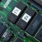
In some process of PCB manufacturing and production of semiconductor chips, both laser and materials require certain amount of heat. Traditional nanosecond lasers generate excessive heat while picosecond and femtosecond lasers can not generate enough heat to remove materials efficiently like PCB repair. Subnanosecond laser provides solution to this problem as its pulse width is between nanoseconds and picoseconds, which takes into account the cool of ultrafast laser and the heat of nanosecond laser. Additionally, in some industries, customers prefer subnanosecond laser due to its competitive cost and good performance.