
Over the years, the government has introduced policies to support the development of laser industry such as encouraging companies to master core technologies through independent innovation, promoting the integration of laser technology and high end manufacturing and establishing a complete laser manufacturing industry system. As a result of these policies, the sales volume of UV nanosecond lasers has continued to increase.
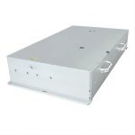
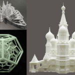
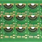
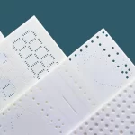
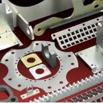
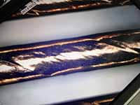
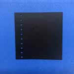
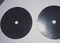
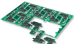
Currently, UV nanosecond lasers are available in the market with power output ranging from 3W, 5W, 10W, and up to 30W and 40W. The technology of 3W, 5W and 10W UV nanosecond lasers are stable and 3W and 5W UV nanosecond lasers are mainly used for applications such as laser marking and 3D printing. The UV nanosecond lasers over 10W power output are applied for thin, hard, and brittle materials such as wafers, silicon wafers and sapphire cover glass. It is a reliable and ideal tool for cutting, etching, punching, scribing of heat sensitive thin film materials, solar cells, FPCB, FPC and PBC.
UV nanosecond lasers still encounter some challenges.
On one hand, 15W and higher power UV nanosecond lasers are still limited by foreign laser giants as there remains large gap on the same type of products in terms of stability, performance and industrial production, which leads to high prices and limited application scenarios. Domestic manufacturers are keeping on the long journey of catching up and gradually approaching the world’s advanced level.
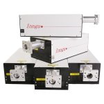
On the other hand, ultrafast lasers such as picosecond and femtosecond lasers have rapidly developed and are now mass produced for commercial use. High power picosecond and femtosecond laser with ultra narrow pulse width have superior processing effects and higher efficiency and can process most materials including metal, semiconductor, glass, sapphire, ceramics, polymer, composite material, thin film, ITO film, solar cells and etc. Unlike femtosecond laser, picosecond laser does not need to expand and compress pulses for amplification. So the design of picosecond lasers is relatively simple, more cost effective and more reliable in performance. For example, when the pulse width is about 10 picoseconds, a very ideal laser “cold” processing result can be achieved via the pulse of ultrafast laser like smaller processing size and higher processing accuracy.
At present, developed countries have basically completed the upgrading of traditional crafts with laser processing in the manufacturing process of major large scale manufacturing industries and have entered the era of “light”. As the world’s largest manufacturing country, China has relatively low penetration rate of laser applications and is still in the growth period. With the rapid development of various industries, the need for industrial upgrading and influence of macro policies are conducive to the continuous release of market demand for UV nanosecond laser and further expansion of the scale of industrial applications.
With the vigorous development of new energy, display panels, consumer electronics, integrated circuits, semiconductors, 5G, big datas and other industries, it is necessary to process a large number of hard, thin and heat sensitive materials such as glass, silicon wafers, sapphire substrate materials, battery poles, PI films, PFC and etc., which are the fields applicable for UV nanosecond laser. In order to achieve the goal of less carbonization and higher efficiency, middle and high end UV nanosecond laser has become more popular in the market. Laser manufacturers are continually innovating in technology, exploring the UV nanosecond laser of higher frequency, narrower pulse width and higher power to find new growth opportunities.